Qualification of Backside Via Etch Process in GaN-on-SiC HEMT Devices
Frank Fan, Minkar Chen, Daniel Hou, and David Wang
Global Communication Semiconductors, LLC. Torrance, CA 90505
GaN-based devices offer significant advantages for next generation military and commercial applications due to its high breakdown voltage and high electron mobility.GaN-on-SiC HEMT device performance andmanufacturing technology have received considerable R&D efforts in recent years. Developing a stable and reliable backside via etch process is one of the key challenges for achieving high performance andhigh yield GaN-on-SiC HEMT devices. In this paper, we report the results of our qualification of the backside fabrication process.
The backside vias are dry etched through the 75m-thick SiC substrate and metalized with electroplated gold. To fabricate the backside vias, the wafer goes through a series of backside processing steps, such as wafer bond, thinning, SiC via etch, GaN etch, and metallization. In particular, the via etch process involves two steps. In the first step, the vias are etched through the SiC substrate in an inductively coupled plasma (ICP) reactor to stop at the GaN buffer layer. In the second step, the vias are etched through the GaN buffer layer in another ICP reactor to expose the frontside metal. Then the vias are metalized with electroplated gold.
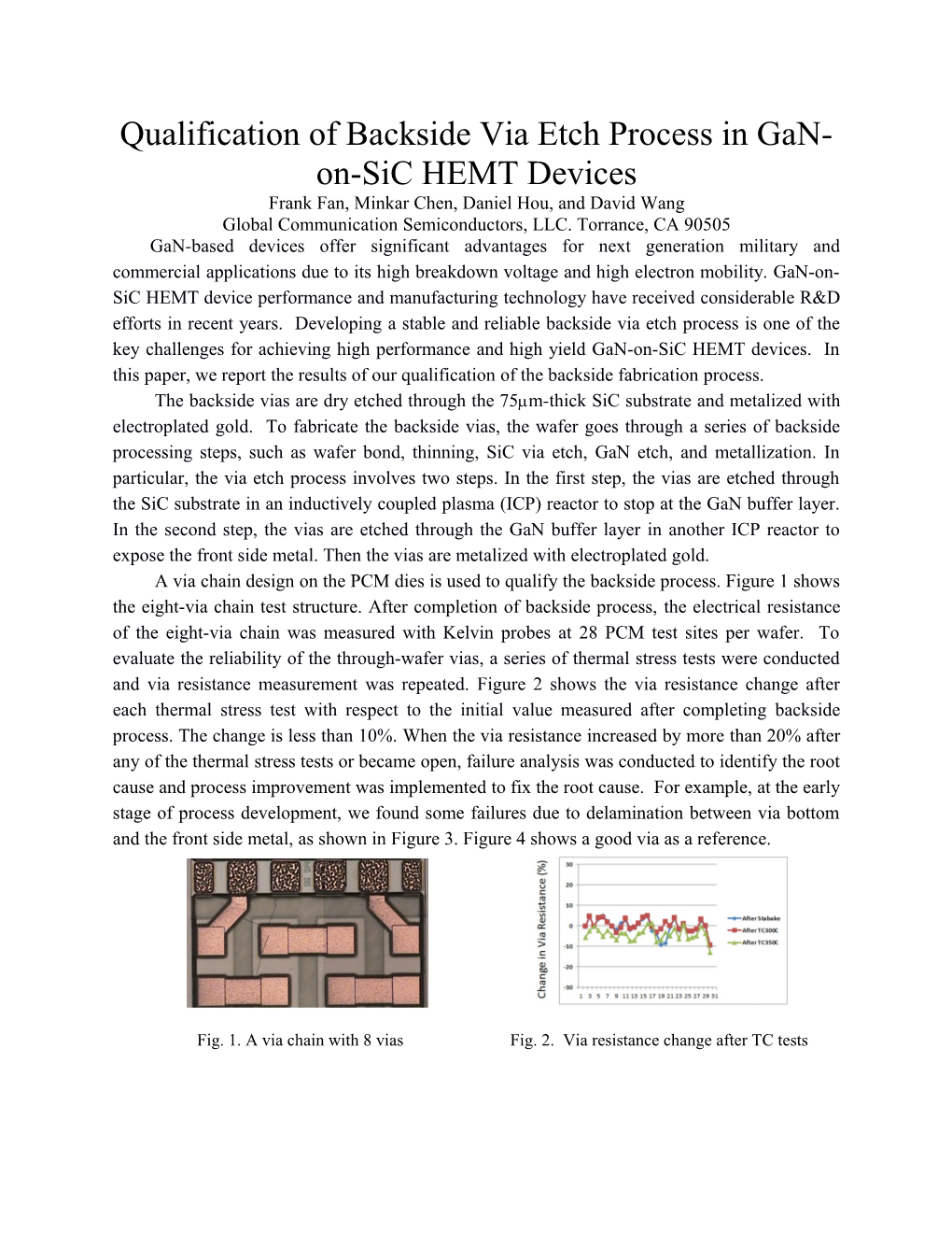
A via chain design on the PCM dies is used to qualify the backside process. Figure 1 shows theeight-via chain test structure. After completion of backside process, the electrical resistance of the eight-via chain was measured with Kelvin probes at28 PCM test sites per wafer. To evaluate the reliability of the through-wafer vias, a series of thermal stress tests were conducted and via resistance measurement was repeated. Figure 2 shows the via resistance change after each thermal stress test with respect to the initial value measured after completing backside process. The change is less than 10%. When the via resistance increased by more than 20% after any of the thermal stress tests or became open, failure analysis was conducted to identify the root cause and process improvement was implemented to fix the root cause. For example, at the early stage of process development, we found some failuresdue to delamination between via bottom and the frontside metal, as shown in Figure 3. Figure 4 shows a good via as a reference.
Fig. 1. A via chain with 8 vias Fig. 2. Via resistance change after TC tests
Fig. 3. Delamination at via bottom and sidewall Fig. 4. A good via as reference
Once the root cause for the failure was identified, new method for via cleaning was implemented to remove the polymer on via sidewall and residues at the bottom of the via more effectively. Figures 5 and 6 show the via before and after the new process was implemented. Results on elemental analyses of the via before and after cleaning will be reported in more details.
Fig. 5. SEM photo of a via with polymer on sidewall Fig.6. SEM photo of a via with polymer removed
A backside process, including etch of round vias has been successfully developed and qualified for the fabrication of 0.5 µm GaN-on-SiC HEMT and MMIC devices.In more advanced designs, slot vias are desired so that the backside ground vias can beplaced under every source pad to reduce source inductance, which would improve RF performance of large GaN HEMT transistors, especially for high frequent operations. Using the same approach, a slot via etch process has also been qualified. Figure 7 shows a SEM photo of the slot via and Figure 8 shows the test results of 5 chips. More details of the test methods and results will be reported in the full manuscript.
Fig. 7. A SlotVia Fig. 8. Via resistance change after thermal stress tests
