Chapter 3 : Fabrication of CMOS Integrated Circuits
This section gives an overview of the integrated circuit technology. Semiconductor devices and circuits are formed in thin slices of a material (called a wafer) that servers as the substrate. For proper operation of the device/circuit, the substrate material must have crystalline structure where all the atoms are aligned in a specific pattern. In the first section of this chapter, the structure and growth of crystals are discussed. The next section deals with the cleaning of wafers which is an important step in the fabrication of integrated circuits. One of the basic building blocks in integrated circuit processing is the ability to deposit thin films of material. A large number of deposited films by wide variety of techniques are used in integrated circuits. These films can either be grown on semiconductor or deposited by various techniques. Most films can be formed by more than one method. Thermal Oxidation of Silicon is taken up first because it is an important step which is often repeated throughout the IC fabrication. This is followed by other principal film deposition techniques such as vacuum evaporation, sputtering and chemical vapor deposition. The properties of the films or substrate can be modified by process like diffusion and ion implantation and they enables to form a variety of devices in integrated circuits. A brief description of diffusion and implantation process and systems are given in section 4. In the subsequent section the lithography process is treated. The basic approaches to CMOS fabrication such as the p-well, the n-well, the twin tub and silicon on insulator processes are discussed in section 6. Very brief discussion on the fabrication of passive components also included. This chapter ends with a discussion on latch up and technology related CAD issues. In summary, an integrated circuit process is usually a structured sequence of operations such as the ability to deposit/modify thin films on the substrate, to apply a patterned mask on the films by photolithographic process, and to etch the films selectively to form actual devices.
3.1 Crystals and Growth
The basic semiconductor materials used in chips are crystalline silicon. This section briefly discuss about the properties of semiconductor crystals and how silicon crystals are grown.
3.1.1 Crystals
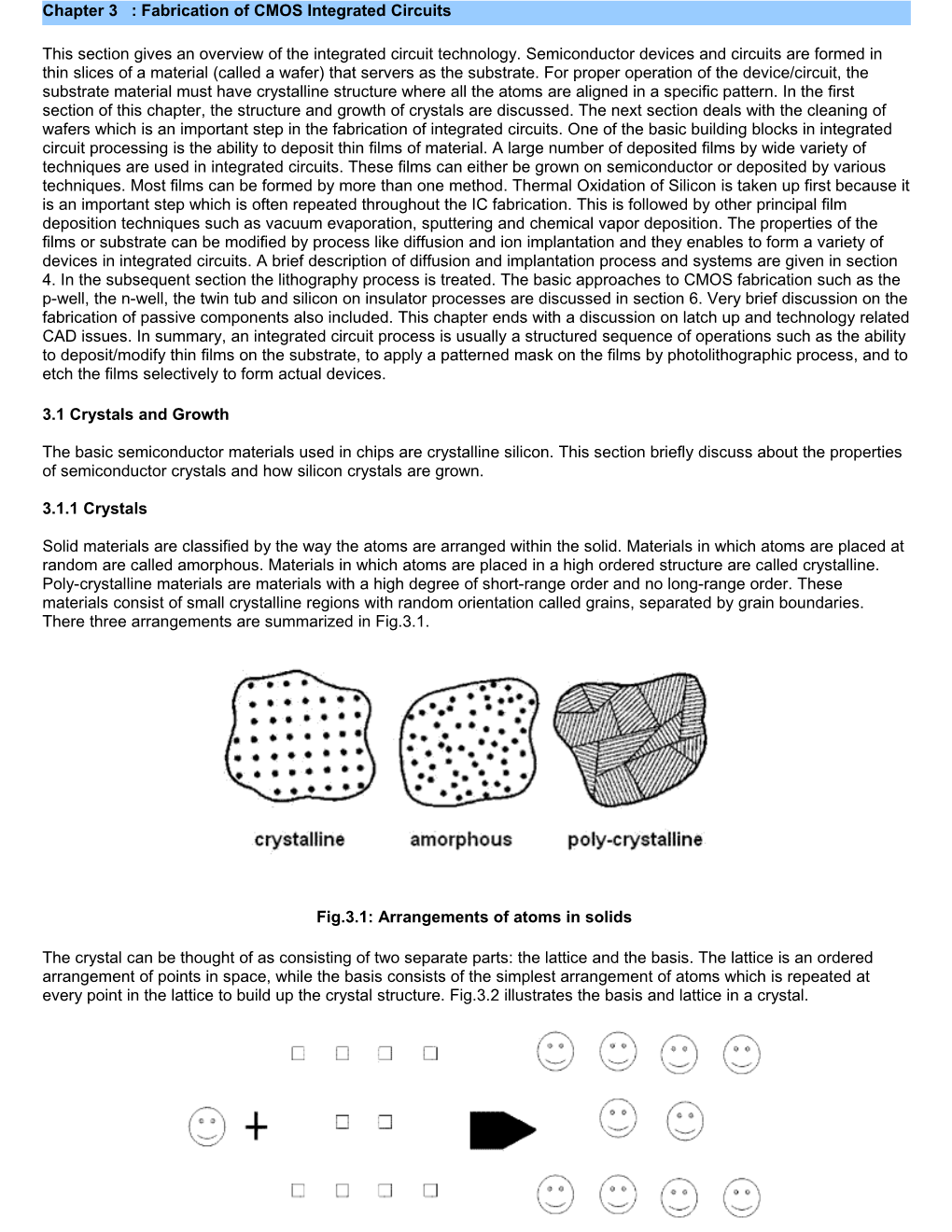
Solid materials are classified by the way the atoms are arranged within the solid. Materials in which atoms are placed at random are called amorphous. Materials in which atoms are placed in a high ordered structure are called crystalline. Poly-crystalline materials are materials with a high degree of short-range order and no long-range order. These materials consist of small crystalline regions with random orientation called grains, separated by grain boundaries. There three arrangements are summarized in Fig.3.1.
Fig.3.1: Arrangements of atoms in solids
The crystal can be thought of as consisting of two separate parts: the lattice and the basis. The lattice is an ordered arrangement of points in space, while the basis consists of the simplest arrangement of atoms which is repeated at every point in the lattice to build up the crystal structure. Fig.3.2 illustrates the basis and lattice in a crystal.
Fig.3.2 : Illustration of basis and lattice in a crystal
A crystal structure is composed of a unit cell, a set of atoms arranged in a particular way and is periodically repeated in three dimensions on a lattice. The unit cell is given by its lattice parameters, the length of the cell edges and the angles between them. In 1848, Auguste Bravais demonstrated that there are in fact only fourteen possible point lattices and no more. In a cubic system, the lattice parameter is the side length of a cube and angles between the edges are 90. The cubic lattices are an important subset of these fourteen Bravais lattices since a large number of semiconductors are cubic. The three cubic lattices are the simple cubic lattice, the body-centered cubic lattice and the face-centered cubic lattice as shown in Fig.3.3. The positions of the atoms inside the unit cell are described by the set of atomic positions (x, y, z) measured from a lattice point.
Fig.3.3 : Atomic arrangements in a basic cubic cell
In Simple Cubic (SC) structure, atoms lie on the corners of a cube as shown in Fig. 3.3a. Very few crystals exhibit this structure. For example polonium exhibits this structure over a narrow range of temperatures. In this structure each atom has six equidistant nearest neighbors.
In Body centered Cubic (BCC) structure, structure atoms lie on the corners of a cube with an additional atom at the centre of the cube as shown in Fig. 3.3b. Its atomic positions are (000), (100), (010), (001), (101), (110), (011), (111) and ( , , ). Metals like Molybdenum, tantalum (Ta) and tungsten (T), iron (Fe), Platinum (Pt), Sodium (Na) and Potassium (K) have this structure. In this structure each atom has eight nearest neighbours. By placement of an atom at the center of the cube, the body-centered cubic structure has twice the atom density of the simple cubic lattice.
In Face centered Cubic (FCC) structure, atoms lie on the corners of a cube with additional atoms at the centers of each cube face as shown in Fig. 3.3c. Its atomic positions are (000), (100), (010), (001), (101), (110), (011), (111), (, , 0), (, 0, ), ( 0, , ), , , 0), (, 1, , 0) and (1, , ). In this structure each atom has twelve equidistant nearest neighbours. Due to its low energy, FCC is extremely common and the examples are lead (Pb), aluminum (Al), copper (Cu), and gold (Au).
Metals which are BCC (like chromium) usually harder and less malleable than close-packed metals such as gold. When the metal is deformed, the planes of atoms must slip over each other, and this is more difficult in the BCC structure.
Fig.3.4 : Diamond Structure
The most common crystal structure among frequently used semiconductors such as silicon and germanium is the diamond lattice, shown in Fig.3.4. Each atom in the diamond lattice has a covalent bond with four adjacent atoms, which together form a tetrahedron as given in Fig.3.4b. The tetrahedral radius of the silicon atom is 1.18 Å. The misfit factor of an impurity atom shows whether it is smaller or larger than the silicon atom. The diamond lattice can also be formed from two face-centered-cubic lattices, which are displaced along the body diagonal of the cube by one quarter of that body diagonal as shown in Fig.3.4c. The violet color atoms are from the second FCC lattice.
Fig.3.5 : Zincblende (ZnS) Structure
Compound semiconductors such as GaAs and InP have a crystal structure that is similar to that of diamond. However, the lattice contains two different types of atoms. This structure is referred to as the zinc-blende lattice, named after zinc-blende (ZnS) and is shown in Fig.3.5, where the two different colors are showing different elements.
Another important geometric feature of a crystal structure is the nearest distance between atom centers (often called the nearest-neighbor distance). This distance is a for the SC lattice, (half of a body diagonal) in the BCC lattice, and (half of a face diagonal) for the FCC lattice.
Example 1: Calculate the maximum fraction of the volume in a simple cubic crystal occupied by the atoms. Assume that the atoms are closely packed and that they can be treated as hard spheres. This fraction is also called the packing density.
The atoms in a simple cubic crystal are located at the corners of the units cell, a cube with side a. Adjacent atoms touch each other so that the radius of each atom equals . There are eight atoms occupying the corners of the cube, but only one eighth of each is within the unit cell so that the number of atoms equals one per unit cell. The packing density is then obtained as follows:
Note that in the case of a SC, about half the volume of the unit cell is occupied by the atoms. The packing density of four cubic crystals is listed in the Table 1.
Table1 : The packing density of four cubic crystals
Radius / Atoms/unit cell / Packaging density
Simple Cubic / / 1 /
Body centered Cubic / / 2 /
Face centered Cubic / / 4 /
Diamond / / 8 /
All lattice planes and lattice directions are described by a mathematical description known as a Miller Index. In the cubic lattice system, the direction [hkl] defines a vector direction normal to surface of a particular plane (hkl). Miller indices are referenced to the crystallographic axes of a crystal. Cubic lattices need only three axes and they correspond to the x, y, z, axes in cubic lattice structures.
Fig.3.6 Intersections of a plane on the x , y and z axis
Intersections of a plane and the x , y and z axes, as shown in figure 3.6, are used to determine the Miller indices of the plane. The Miller Indices h, k, l are obtained as follows:
Determine the points at which a given crystal plane intersects the three axes, for example at (a, 0, 0), (0, b, 0), (0, 0, c). If the plane is parallel an axis, it is said to intersect the axis at infinity.
The Miller index for the face is then specified by (1/a, 1/b, 1/c), where the three numbers are expressed as the smallest integers (common factors are removed). Negative quantities are indicated with an over bar.
Example 2:
A plane intersects the crystallographic axes at (2, 0, 0), (0, 3, 0), (0, 0, 4).
Step 1: (1/2, 1/3, 1/4); multiply by 12 to express as smallest integers.
Step 2: (6, 4, 3) are the Miller indices. This is a (643) plane.
The (110) is the plane intersects the crystallographic axes at (1,0,0), (0,1,0) and (0, 0, ). z=infinity means that this plane does not intersect the z axis.
Use the [ ] notation to identify a specific direction (i.e. [101]).
Use the < > notation to identify a family of equivalent directions (i.e. <110>).
Use the ( ) notation to identify a specific plane (i.e. (113)). Use the { } notation to identify a family of equivalent planes (i.e. {311}).
A bar above a index is equivalent to a minus sign.
Fig.3.7: Different crystallographic planes in a cubic system
Fig.3.7 shows the different crystallographic planes in a cubic system. The separation between adjacent planes in a cubic crystal is given by
The separation between set of (111) planes is the smallest compared to {110} and {100}.
For cubic crystals, the angle, between two planes, ( h1 k1 l 1 ) and ( h2 k2 l 2 ) is given by:
Example 3: Calculate the angle between the (111) and (200) planes.
From the above equation,
which produces the result, = 54.75
In a similar way one can find the angle between any planes and the values of most common planes are summarized in the Table 2.
Table 2 : The angle between planes in cubic crystals
Planes / 100 / 110 / 010 / 001 / 101
100 / 0.00 / 45.0 / 90.0 / 90.0 / 45.0
011 / 90.0 / 60.0 / 45.0 / 45.0 / 60.0
111 / 54.7 / 35.3 / 54.7 / 54.7 / 35.3
Linear density of atoms can be defined as number of atoms centered on a direction vector / length of direction vector. Similarly planar density of atoms is number of atoms centered on a plane / area of plane. Linear density and planar density are important considerations during deformation and "slip"; planes tend to slip or slide along planes with high planar density along directions with high linear density. Based on these values {111} planes have the following unique characteristics:
The crystal growth is easiest
The chemical etching is slowest
Tensile strength is highest
Modulus of elasticity is highest
It is the typical cleavage plane
Cross sectional view Top View
Fig. 3.8 : V-groove etching in (100) silicon showing the exposed {111} sidewalls
An anisotropic wet etch on a silicon wafer creates a cavity with a trapezoidal cross-section as shown in Fig. 3.8. The bottom of the cavity is a <100> plane, and the sides are <111> planes. The white material is an etch mask, and the grey material is silicon. The angle between (111) planes and (100) surface is 54.7° as calculated before and the etching stops at (111) planes at this angle resulting a V-groove.
Example 4 : Calculate the density of Si from the lattice constant, atomic weight, and Avogadro's number. Recall: Avogadro's number (6.02 × 10²³ ) is the number of molecules/atoms in a gram molecular weight of a substance. Lattice constant = a = 5.43 x 10⁻⁸ cm
How many Si atoms in the diamond cell?
8 corner atoms x (1/8) = 1
6 face atoms x (1/2) = 3
+ 4 interior atoms = 4
Total 8 atoms/unit cell
The number of atoms/cm3 = 8/a3
= 8 / (5.43 X 10⁻⁸ cm)3
= 4.996 x 10²² atoms/cm3
If 6.02 x 10²³ silicon atoms make 28.1g; then 4.996 x 10²² atoms should weigh 2.332 g. Thus the density of silicon is 2.332 g/cm3.
Up to the 150 mm wafer diameter era, wafers had flats, and the flats indicate the following information:
1. The doping type of the wafer (n- or p-type)
2. The orientation of the wafer: {100} or {111}
And wafers with diameters larger than 200 mm generally will have no flat at all, but just a small "notch" as shown in Fig. 3.9.
Fig. 3.9 Identification of wafers
By measuring the sign of the thermo voltage between a hot tip (a soldering iron) and a room-temperature tip pressed on the wafer can indicate whether the wafer is n- or p-type.
The breaking (cleaving) of wafer indicate the orientation of a wafer; e.g. {100} wafer pieces will be rectangular.
In this section we have studied about different types of cubic crystal structures, packing densities, various crystal planes and directions, miller indices etc. In the next section we will study how the crystals are made.
Chapter 3 : Fabrication of CMOS Integrated Circuits